Facilities
Wafer production tools
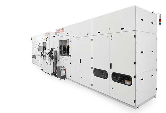
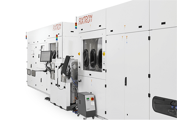
GaN MOCVD growth tool
Our GaN HEMT growth tool is a production-scale metal organic chemical vapor deposition (MOCVD) reactor for growth of III-V nitrides on SiC and Si wafers sized ≤ 8’’.
Fabrication tools
LITHOGRAPHY TOOLS
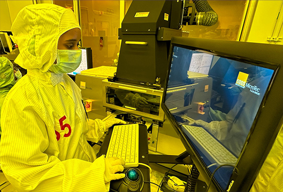
We have a comprehensive tool set to meet lithographic requirements, including a contact mask aligner (i-line, with top and bottom alignment capabilities), a deep ultraviolet (248 nm KrF excimer laser) stepper coupled with an automated resist processing station, and a production-grade 100-kV e-beam lithography system to obtain critical dimensions downwards of 50 nm across 4” and 6” wafers.
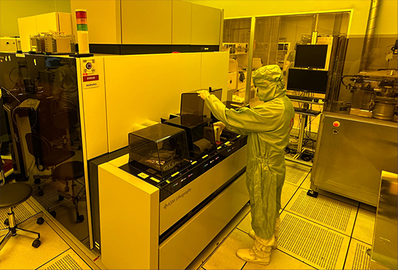
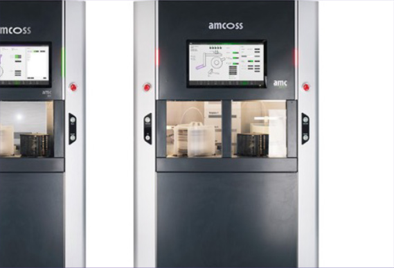
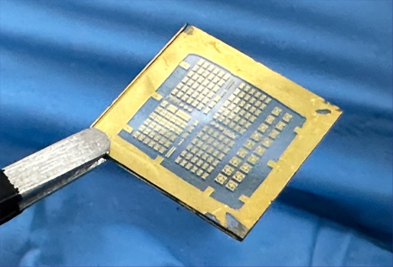
DEPOSITION TOOLS
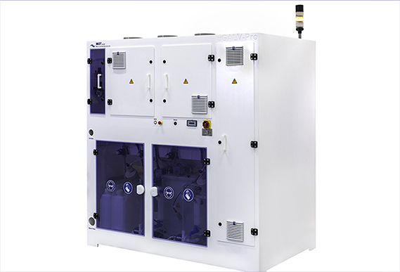
Our metal deposition tools include e-beam evaporators and sputtering systems that can handle ≤ 8” wafers and can deposit Ti, Al, Ni, Au, W, Cu, Ni, Cr, and Ta. Our dielectric deposition tool line is served by sputtering, plasma enhanced chemical vapor deposition (PECVD), and atomic layer deposition (ALD; thermal and plasma enhanced) tools capable of handling a variety of oxide and nitride layers. Our electroplating tool for thick metal layers has independent processes for the single-side plating of Au, Ni, and Cu on ≤ 8” wafers.
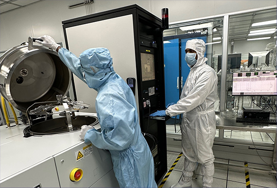
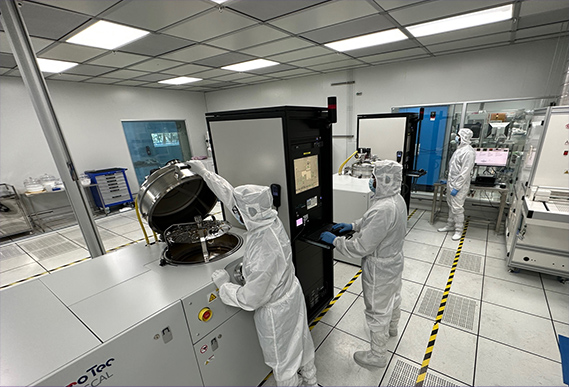
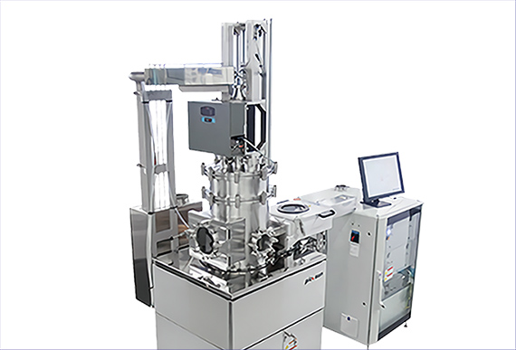
ETCHING TOOLS
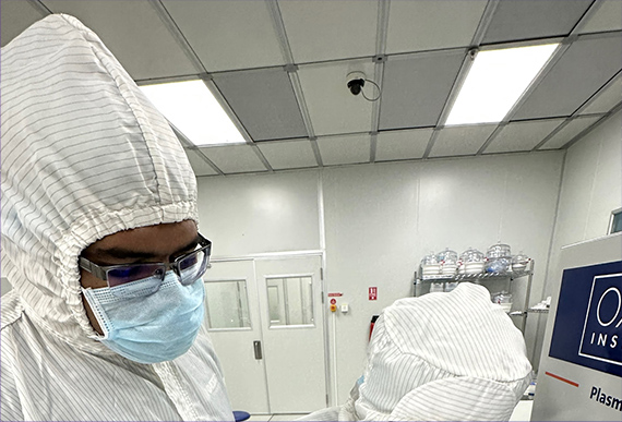
We have a range of tools capable of resist strip/plasma ashing and etching of GaN, AlGaN, SiC, metal, SiOx, and SiNx (≤ 6”) to cater to the diverse needs of GaN device processing. Our dedicated 4”- and 6”-GaN etching tools can perform atomic layer etching to yield an excess surface roughness of ≤ 1 nm. The tools are also capable of etching feature sizes ≤ 100 nm and creating tunable etch profiles to cater to a wide range of process requirements. SiC is one of the hardest materials to etch; we have a dedicated ICP-RIE tool to achieved deep aniostropic SiC etching. All our tools are monitored for stability and repeatability to achieve the best process quality.
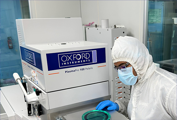

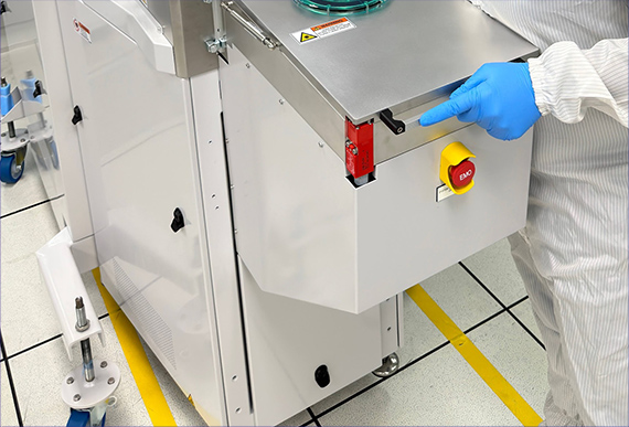
ANNEALING TOOL
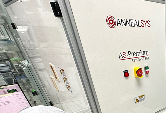
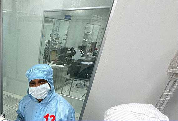
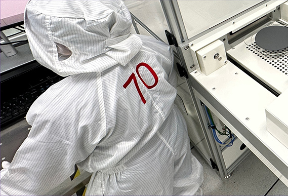
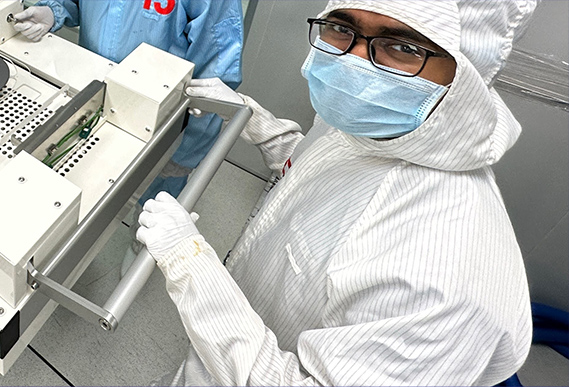
Our rapid thermal processor (RTP) is capable of handling 4’’ and 6’’ wafers at annealing temperatures up to 1200°C across 6’’ substrates.
Characterization tools
PROCESS CHARACTERIZATION TOOLS
Ellipsometer
Process characterisation is key to achieving repeatable and scalable fabrication. We use dedicated in-line characterisation tools to perform qualification between process steps and thereby achieve the best process integration quality. Our spectroscopic ellipsometer is a powerful optical characterisation tool that can measure the thickness of deposited and etched layers. It can measure and map thickness and optical constants across 4” and 6” wafers.
Surface Profilometer
Our surface profilometer measures the thickness of optically opaque materials, such as metals. It also measures the topography developed during device processing.
Optical Microscope
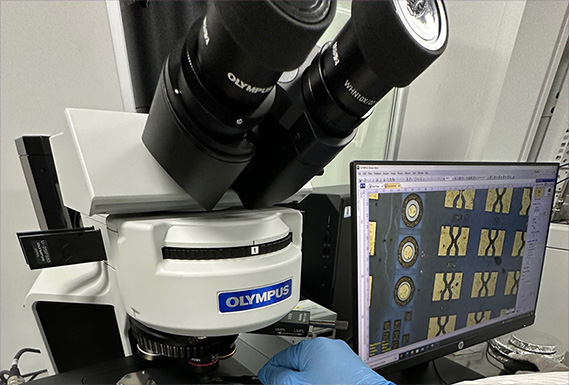
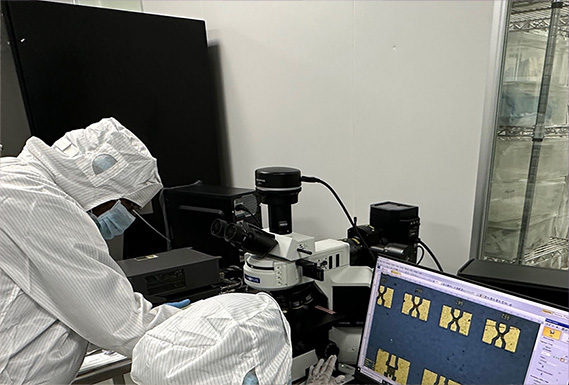
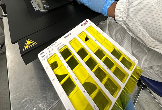
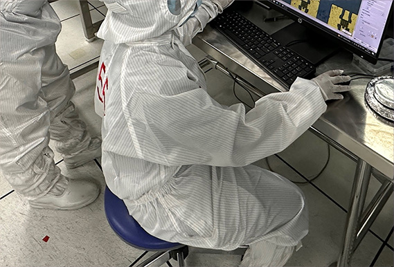
Our optical microscope has both transmission and reflectance geometries, along with high-end image analysis options, as well as fluorescence geometry.
ELECTRICAL CHARACTERIZATION TOOLS
Setup 1: On-Wafer Manual DC Measurements
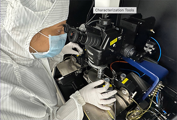
Our on-wafer manual DC measurement setup provides an on-wafer probing solution for substrates up to 150 mm. The setup can perform DC characteristics of the device under test upon integration with a semiconductor device analyzer. It supports I-V, C-V, resistivity and many more test modules, with applications ranging from basic to cutting-edge. The probe station in this setup has a thermal chuck system with a temperature range of 30 ºC to 200 ºC.
Measurement capabilities:
- Id-Vd
- Id-Vg
- Ig-Vg
- Contact and Sheet resistance
- C-V
- OFF state leakage
- MESA leakage
- Temperature dependent I-V
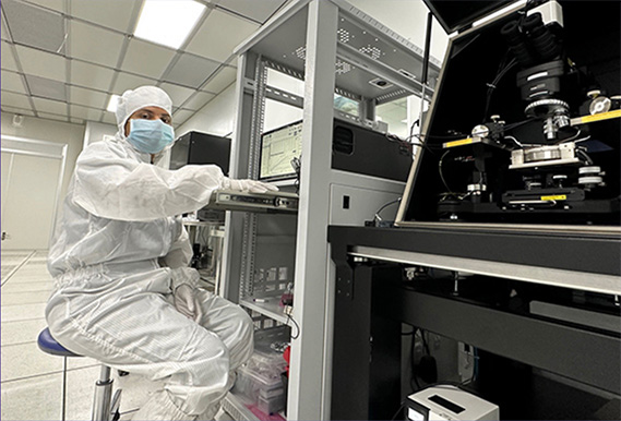
Setup 2: High/Medium/Low Power DC Measurements
Semi-automatic DC measurements:
The tool is a semi-automatic probe station with 150 mm chuck inside the microchamber that isolates and shields the chuck from external environment. This enables ultra-low noise measurements. Hi-ISO Coaxial Chuck with max. breakdown voltage of 500 V. The probe station is integrated with 4200A SCS parameter analyser, 2657A high voltage SMU, 2635B low current SMU, 2651A high current SMU, and 7072-HV semiconductor matrix card that enables low/medium power measurements.
High power DC measurements:
The tool is a high-power manual probe station with 6-inch chuck. It is housed with high voltage, high current triaxial probe arms and probe tips assembly. The probe station is integrated with Keithley high voltage and high current SMUs for high power measurements.
Measurement capabilities:
1) Ids-Vds:
- Low – high voltage (> 1500 V)
- Low – high current (≤ 100 A)
- Pulse width: 150 μs to DC
- Nanosecond pulse down to 120 ns
2) ON and OFF state breakdown measurements
3) Igs-Vgs for low voltage/current
4) Ids-Vgs:
- Low – medium voltage
- Low – medium current
5) Cg/Cd Vs Vg/Vd with capacitance measurement resolution of 1aF
6) Capable of on-wafer measurements of devices that are ready for packaging
7) Automation and auto parameter extraction module
8) High power device measurements
9) Device reliability: HCI, TDDB, NBTI, etc.
10) Automatic wafer-level device reliability measurements
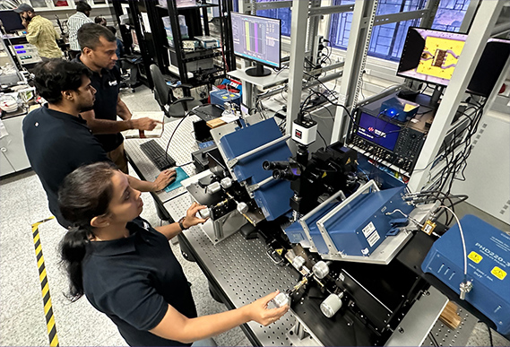
Setup 3: Non-Linear RF Device Characterization
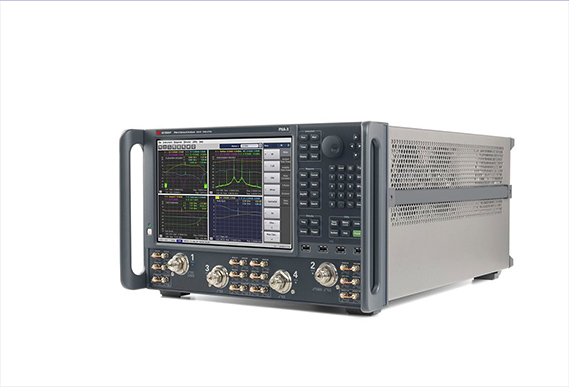
The non-linear RF device characterization setup has harmonic pulsed loadpull capability that enables the nonlinear RF characterization of active devices operating in the 1.8–67 GHz frequency range. This is an integrated setup containing an RF probe station, a vector network analyzer, source and load tuners, a pulsed IV system, and an RF pulse modulator.
Measurement capabilities:
- On-wafer and connectorized loadpull measurement with pulsed bias and pulsed RF capabilities
- IMD measurement
- Harmonic loadpull (up to 3rd harmonic at load)
- AM/AM and AM/PM distortion
Setup 4: Pulsed IV and Small Signal RF Characterization
This setup is capable of performing connectorized as well as on-wafer pulsed IV and pulsed S-Parameter measurements of RF devices. For on-wafer testing, the probe station has a thermal chuck system with a temperature range of 30–200 ºC. The setup allows device modeling across entire linear and nonlinear operating ranges.
Measurement capabilities:
- Pulsed IV measurement with pulsed width down to 200 ns
- Pulsed S-parameter measurement with pulsed width down to 3 µs
Compact modeling of GaN HEMT using the IVCAD modeling software
Packaging tools
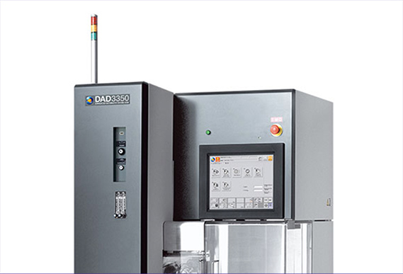
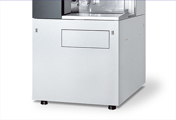
Wafer dicer
Our ultrasonic-wave dicing machine can handle workpieces ≤ 8’’. It allows the processing of Si and difficult-to-process materials, such as ceramic, glass, and SiC, and can also handle the alignment of multiple mounted workpieces.
Wafer grinder
Our grinding tool is a compact, automatic grinder (wafer-thinning) that can handle workpieces ≤ 8″ in diameter. It is designed to process a variety of materials, such as Si and SiC wafers.
Die bonder
Our die bonder can perform adhesive and eutectic die bonding in automatic, semi-automatic, as well as manual modes. The tool allows die picking from wafers (≤ 8″), waffle packs (2” and 4”), and gel packs (2” and 4”). It allows the attachment of die in the size range of 0.1–30 mm. The fully automatic pick and place capability of the die bonder has an accuracy of 3 µm at 3 sigma.
Wire bonder
Our wire bonder has changeable bond heads, which allow wedge-wedge and ball-wedge bonding of thin, heavy, and ribbon wires in a X: 100 mm/Y: 150 mm/Z: 42 mm working area. Our tool can create heavy and ribbon wire bondheads for 2–24 mil Al, Cu, and AlCu wires and ribbon wire bondheads for 10–80 mil by 1–16 mil Al, Cu, AlCu wires. It can create thin wire wedge-wedge bondheads for Al and Au wires (0.5–3 mil) and Cu wires (0.7–2 mil). It can also form ball-wedge bondheads with 0.7–2 mil Au wires.

Software
Our Advanced design system (ADS) software is an RF and microwave design software that includes ADS Core, EM Design, Layout, RFPro EM Simulator (Momentum and FEM), RF Ckt Sim, Sys-Ckt Verification, and Complete virtual test bench features.
IC-CAP
Our integrated circuit characterization and analysis program (IC-CAP) software is the industry standard software for DC and RF semiconductor device modeling. It includes the WaferPro application for automated wafer-level measurement, a GaN RF Modeling bundle, and a power electronic model generator.
TCAD
Incubates can submit their computational requirements related to our Technology Computer-Aided Design (TCAD) software to GEECI employees, who will perform evaluations on their behalf and share data.
