Deposition Tools
Our metal deposition tools include e-beam evaporators and sputtering systems that can handle ≤ 8” wafers. Our dielectric deposition tool line is served by plasma enhanced chemical vapor deposition (PECVD), and atomic layer deposition (ALD thermal and plasma enhanced) tools capable of handling a variety of oxide and nitride layers. Our electroplating tool for thick metal layers has independent processes for the single-side plating on ≤ 8” wafers.


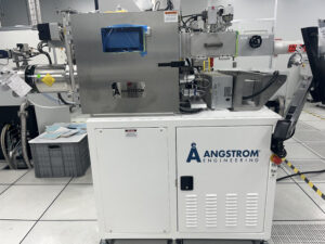
Optimized for highly directional, line-of-sight deposition, this system operates with minimal substrate heating to serve as our primary tool for precision lift-off processes and thick contact metallization. It delivers clean, sharp liftoff edges while maintaining fast cycle times for high wafer throughput.
Our Sputter System delivers excellent step coverage and dense thin films over complex surface topography. It supports reactive sputtering, substrate heating and bias control, allowing for sequential multi-layer deposition without breaking vacuum to eliminate interfacial contamination.
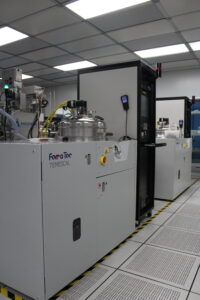
Manufacturer: Annealsys
This rapid thermal processing system enables precise control over tight thermal budgets via ultra-fast ramp rates. Designed for versatility, it is optimized for activating dopants and forming reliable ohmic contacts while delivering highly reproducible, run-to-run process conditions.
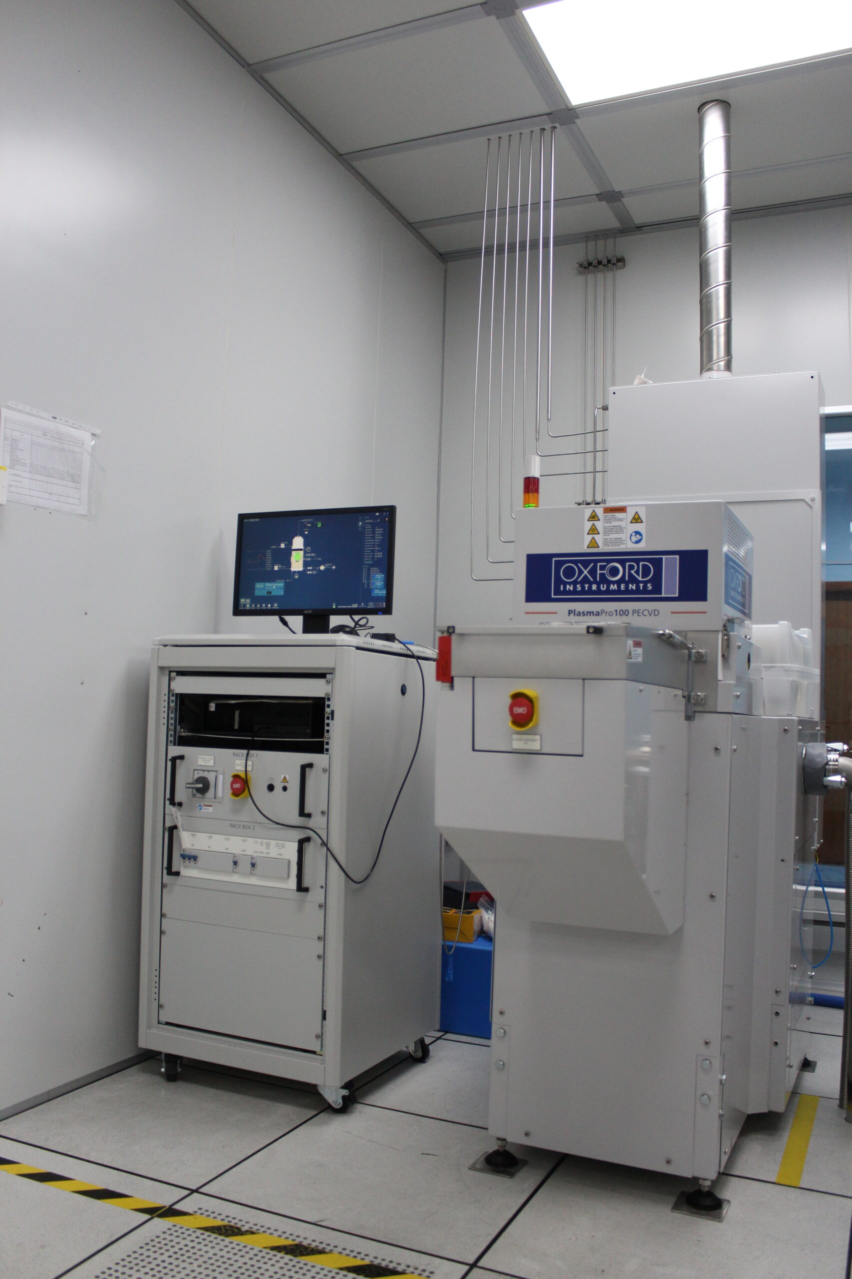
For temperature-sensitive substrates, our PECVD system deposits high-quality dielectric capping, insulation and passivation layers at low thermal budgets. It utilizes dual-frequency RF power to precisely tune film stress and prevent wafer bowing.
Manufacturer: Picosun/AMAT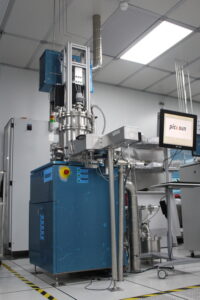
Our plasma enhanced ALD system guarantees ultra-conformal, pinhole-free coatings over extreme aspect ratio features and 3D architectures. It relies on self-limiting monolayer growth to provide absolute thickness control at the angstrom level, making it vital for critical gate oxides and diffusion barriers.

Our Electroplating Station enables high-rate, selective and cost-effective deposition of thick metal layers for power routing, MEMS or advanced packaging structures. It uses precise current-density modulation to prevent void formation, ensuring robust electrical and mechanical structural integrity.
