Etching Tools
We have a range of tools capable of resist strip/plasma ashing and etching of GaN, AlGaN, SiC, metal, SiOx, and SiNx (≤ 6”) to cater to the diverse needs of GaN device processing. Our dedicated 4” and 6” GaN etching tools can perform atomic layer etching to yield an excess surface roughness of ≤ 1 nm. The tools are also capable of etching feature sizes ≤ 100 nm and creating tunable etch profiles to cater to a wide range of process requirements.
SiC is one of the hardest materials to etch we have a dedicated ICP-RIE tool to achieved deep aniostropic SiC etching. All our tools are monitored for stability and repeatability to achieve the best process quality.


Manufacturer: Oxford Instruments 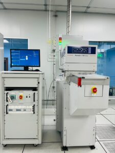
Capable of shaping high-precision vertical profiles, this system delivers highly anisotropic dry etching at the wafer level for dielectrics. It provides high selectivity and uniformity required for critical gate dielectrics and passivation layers in GaN HEMT devices.
Manufacturer: Oxford Instruments 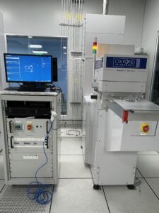
Our GaN Etch system is optimized for high-density inductively coupled plasma (ICP) etching on production-scale GaN wafers. It delivers the smooth sidewalls, precise depth control and high mask selectivity essential for high-yield GaN HEMT fabrication.
Manufacturer: Oxford Instruments 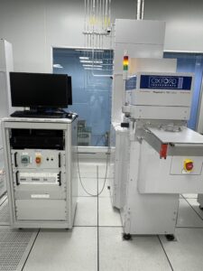
The ALE tool provides precise etch control required for recessed processes, with end pointing capabilities wherever applicable.
Manufacturer: Oxford Instruments 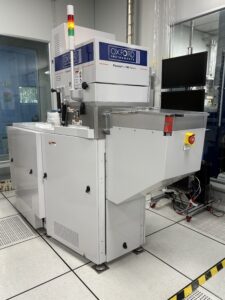
This system delivers the high bias and plasma density needed for etching high aspect ratio trench and through via on Si and SiC substrates.
Manufacturer: Oxford Instruments 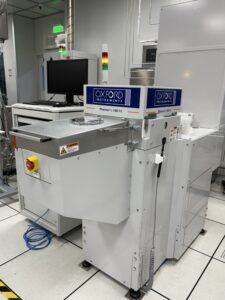
Our Reactive Ion Etching (RIE) system is capable of etching common metals used in semiconductor processing.
Manufacturer: Oxford Instruments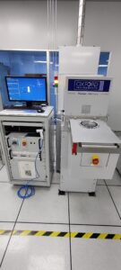
The plasma asher provides highly selective stripping of photoresists and organic contaminants at the wafer level without damaging underlying thin films, allowing for post-etch cleanings, surface descumming and surface activation throughout GaN HEMT process flows.
