Characterization Tools


Inline Characterization
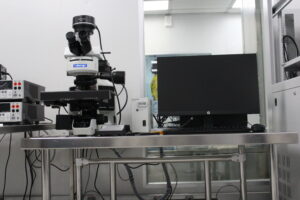
Our optical microscope has both transmission and reflectance geometries, along with high-end image analysis options, as well as fluorescence geometry.
Manufacturer: Sentec Instruments GMBH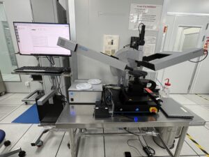
Our spectroscopic ellipsometer is a powerful optical characterisation tool that can measure the thickness of deposited and etched layers. It can measure and map thickness and optical constants across 4” and 6” wafers.
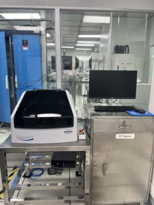
Our surface profilometer measures the thickness of optically opaque materials, such as metals. It also measures the topography developed during device processing.
Manufacturer: Tektronix 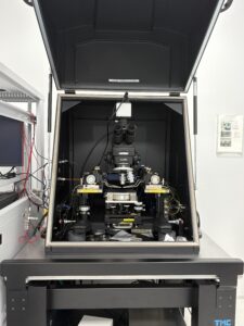
Our inline probe station drives targeted in-line monitoring of wafer-level device parameters such as breakdown voltage, I-V and C-V characteristics.
RF Characterization
Manufacturer: Keysight, Focus Microwaves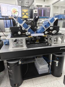
Our advanced RF Load-Pull measurement platform is designed for comprehensive large-signal and non-linear characterization of RF and microwave devices. The system integrates an RF probe station, vector network analyzer (VNA), source and load tuners, DC pulsed I-V instrumentation and an RF pulse modulation system.
Key Capabilities:
-
- Frequency range: 1.8 GHz to 67 GHz
- Continuous and pulsed DC and RF measurements
- Source and load-pull characterization
- Harmonic load-pull measurements up to 3rd harmonic
- Accurate extraction of power, efficiency, gain and linearity performance metrics
Manufacturer: Maury Microwave 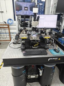
This versatile characterization platform supports both pulsed and continuous DC I-V measurements, along with small-signal S-parameter characterization for on-wafer and connectorized RF devices.
Key Capabilities:
-
- Pulse widths down to 200 ns
- Small-signal characterization up to 67 GHz
- Drain voltage capability up to 250 V
- Drain current capability up to 30 A
- Pulse power capability up to 3 kW
Manufacturer: Customized In-house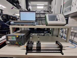
Our RF Manual Load-Pull setup is dedicated to the non-linear characterization of connectorized and packaged RF power devices through manual impedance tuning.
Key Capabilities:
- Frequency range: 0.8 GHz to 8 GHz
- Continuous-wave (CW) output power handling up to 100 W
- Manual source and load impedance tuning
- Characterization of output power, gain, efficiency, and optimum load impedance
This setup provides a flexible and cost-effective solution for RF power amplifier development and performance optimization.
Power Characterization
Manufacturer: Form Factor 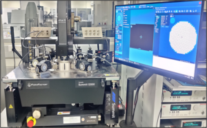
The Cascade Microtech Summit 12K Semi-Automatic Probe Station supports wafer-level measurements on wafers up to 150 mm. It is equipped with a high-isolation coaxial chuck supporting a maximum breakdown voltage of 500 V, enabling ultra-low current measurements in the femtoampere (fA) range. The system can perform wafer-level I–V, C–V and breakdown measurements.
Manufacturer: Everbeing International Inc.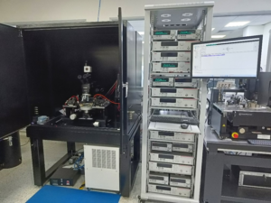
This probe station is equipped with a DC-powered hot chuck with a temperature range from room temperature to 200°C. It accommodates samples ranging from 10 mm × 10 mm die pieces to 6-inch wafers.
The system supports:
-
- High-voltage measurements up to 3 kV
- High-current measurements up to 100 A pulsed
- High-voltage C–V measurements up to 3 kV
The setup includes five micro-positioners with triaxial magnetic bases, enabling stable probing and ultra-low current measurements during high-power characterization.
Software
ADS
Our Advanced design system (ADS) software is an RF and microwave design software that includes ADS Core, EM Design, Layout, RFPro EM Simulator (Momentum and FEM), RF Ckt Sim, Sys-Ckt Verification and Complete virtual test bench features.
IC-CAP
Our integrated circuit characterization and analysis program (IC-CAP) software is the industry standard software for DC and RF semiconductor device modeling. It includes the WaferPro application for automated wafer-level measurement, a GaN RF Modeling bundle and a power electronic model generator.
TCAD
We can perform evaluations for customers using our Technology Computer-Aided Design (TCAD) software.
